
 MENU
MENU Students rewarded for their circuit designs in EECS 413
The course, Monolithic Amplifier Circuits, has a tradition of offering prizes for the top final projects designed by the students.
The course Monolithic Amplifier Circuits (EECS 413), taught by Prof. Michael Flynn, has a tradition of offering prizes for the top final projects designed by the students, thanks to the support of industry. This year Tektronix sponsored the contest.
The course provides introductory as well as advanced topics in CMOS analog and mixed signal design. A full suite of commercial design tools from Cadence is used for schematic entry, simulation, and layout. Designs are implemented in a commercial 0.13μm CMOS process.
This year’s first place team earned $1,500 for their project, Adaptive Bandwidth PLL; the second place team earned $500 for their project, Inductorless Wideband Balun-LNA.
Adaptive Bandwidth PLL

 Enlarge
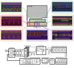 Enlarge
This team designed a 10GHz, 8-phase ring-oscillator based phase-locked loop (PLL) for timing generation in communication applications. The PLL has fast frequency acquisition, an adaptive bandwidth, and the ability to work over a wide range of frequencies using different circuit techniques.
The circuit is implemented in 0.13µm IBM process technology node and achieves 3x better timing resolution (12ps) compared to the FO4 delay (35ps). The circuit takes up approximately 240µm x 210µm of area and consumes 15mW when running at a maximum speed of 10GHz.
Inductorless Wideband Balun-LNA with Noise Cancellation and Gain Boosting
 Enlarge
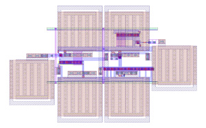 Enlarge
Low noise amplifiers (LNAs) are the critical first components in modern radio receivers. This team designed an inductorless wideband LNA applicable between 400MHz and 2GHz. The design uses cross-coupled common gate stages and a common source stage to achieve simultaneous noise cancellation and gain boosting. The team contributed simple resistance-driven design equations for noise cancellation of all common gate stages.
When simulated with a 0.13µm technology, this design achieved a minimum noise figure of 3.7dB and minimum gain of 17.3dB between 400MHz and 2GHz. Total power consumption was 3.15mW and total area including passives was 0.019mm2. These specifications are competitive with recent published results.